
Canon PowerShot G9
ƒ/2.8
7.4 mm
1/13
80
Puzzle Series: What is this, or what do you want it to be?
(I think this might go quickly, but I’ll leave it open overnight for the most precise answer… =)
Puzzle Series: What is this, or what do you want it to be?
(I think this might go quickly, but I’ll leave it open overnight for the most precise answer… =)
Multicore computer?
The copper devices look like large capacitors, the little rectangles are ceramic capacitors, and the silver squares maybe some coputer chip.
I want it to be a neural network – say with 10E9 processors and 10E11 interconnections. With about 1000 of those connected up, I could build a pretty interesting machine – which would be able to guess at this puzzle
Cut-away model for like an FPGA prototype, router, or telephone switch. Looks too simple to be general-purpose processors. Quite the massive heatsink with springs to apply equal pressure on each thing, whatever it is.
The letters on the little caramel-cubes intrigues me.
This is a bloody great battery composed of lots of smaller Li Ion cells. This is a cut-away model for demonstration purposes. Part of the outer aluminum containing matrix (which also functions as heat conduit) has been removed to show the individual cells (the copper-clad cylinders) – it looks like a quarter of the overall battery has been opened up and that part contained 4-by-4 = 16 cells. The wholle battery contained 4 times 16 plus apparently one in the middle = 65.
Some number of these batteries are connected together to power expensive sports cars.
I’m going with the battery. well, or the super-switch. and those bits of fudge? temperature and current monitors for each cell?
I suspect that Jitze, once again, is correct. Until I saw his response, I was going down the line that these were actuators to control the surface tolerance of a mirror. … but that doesn’t look like a very reflective mirror, and they seem too closely spaced for that function. But that’s what I want it to be! 😉
I’m with the heatsink theory – what look like bare die, intimate thermal contact to copper, the copper in contact with a big old lump of aluminium.
Although the bottom thingie doesn’t look anything like a PCB. But the brown thingies do look like decoupling capacitors. So I’m eager to see the answer.
Hang on – just noticed that where one of the ‘brown thingies’ is missing there is a regular ball grid, so they are not capacitors. But the presence of balls on the bottom matrix does stack up with the mirrored thingies being bare die, placed pad down onto a ball grid.
But basically I’m thrashing so I give up!
For the missing parts, looks like old… is it one member of your Core Memory board collection?
Spring-loaded heat pipes (Cu) and heat-spreader (Al) to pull heat from an MCM module (CPU?). Those are almost certainly flip-chip IC’s (perhaps just power transistors) with bypass caps throughout. It’s a non functional cut-away unit (obviously). Without knowing scale (and hence how thinly they were back-ground), it’s a lot harder to guess. If they’re thick, perhaps they’re SiC or GaN devices but I’m sticking with Si based on color.
Perhaps those columns are not just copper, but beryllium copper. Part of the cooling mechanism for a cryogenic quantum computer.
I also think those are integrated circuits of some sort, with an unusual copper and aluminum heatsink arrangement. To me, the chips scream short-run fabrication and large heat production- hence the unlabeled, slightly rough bare dies. This board cost a fortune to produce.
I suspect liquid cooling, since there seems to be a lot of focus on thermal conductivity, but not so much on dissipation surface area.
I don’t think they’re power control chips- no big fat power traces. I also suspect their bus bandwidth needs are fairly modest- there’s not enough room for wide, high-speed busses between the chips. That makes me think of relatively simple but massively computationally intensive problems, especially codebreaking.
The board looks strange to me, but I don’t think it looks like a completely modern fabrication technique.
Final answer: This is part of a codebreaking machine.
Detail guesses: Government funded, at huge expense, and made in secret. Liquid nitrogen cooled. Decommissioned and declassified, maybe from the 80’s. Made to break DES. This is just a small part; there were probably hundreds or thousands of cores total.
It’s fun to see 24 hours of comments, and many correct guess elements (acknowledged below).
This is a historical artifact that I just received from an IBM exec that shows the trailing edge of an important industry transition – from bipolar to CMOS transistors for logic.
Here you can see the effort expended to manage heat dissipation for the processor core of an IBM 370-3081 high-end mainframe, which shipped 1981 to 1987.
The package is called the “thermal conduction module”, code-named FS for “Future System”. Here is the image IBM has in its archives:
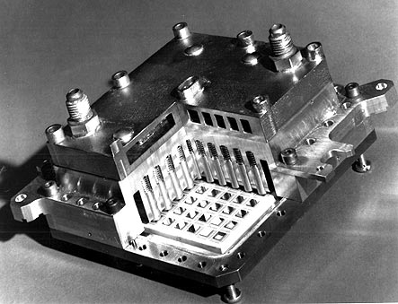
My photo is from a similar display unit that one of the designers kept, with the aluminum cut away to see the innards.
24 metal modules like this made up the processor, 460,000 logic circuits in total.
Each chip contained distinct bipolar logic. The similar size of the chips was dictated by heat concerns, not manufacturing yield maximization, or a pattern of repeating design elements.
Each chip dissipated up to 32 watts (think the surface of an iron). The heat sink pistons were spring-loaded to make a good thermal contact with the backside of the flip chips. The open space around them was filled with helium for additional heat transfer (the entire aluminum case is hermetically sealed).
The chips are mounted on a 32- layer ceramic board with 350,000 vertical via holes for interconnect. I notice a number of little yellow wires as well (if they are hand soldered repair wires, they are not even visible with the naked eye) . On the backside of this module are 1,800 pins which needed a zero-insertion force approach to mate with the backplane.
The processor complex was driven by a 400 Hz AC power rail and cooled with heat exchangers in a closed loop of chilled water, with two water pumps.
All of this gets summarized by IBM marketing as “advanced new technology for processor unit logic.”
IBM believed they would take a ~10x performance penalty by switching to a more power efficient CMOS platform, and so they took the older bipolar technology through some extreme contortions. But ultimately, these heroic approaches did not scale for bipolar, and the steady march of Moore’s Law brought the scalable CMOS processor to the forefront. For now.
Bingo to many for first identifying key elements:
Brewbooks – “multicore computer”, right out of the chute… but only dual core.
Cmlburnett – “cut-away model” and “massive heatsink with springs to apply equal pressure on each thing”
Ramones – “ball grid” of “bare die”
Alieness – “old” and related to my “core memory board collection”
Posamentier – “MCM module (CPU)” with “Si”
AMagill – “This board cost a fortune to produce.” And correct that some extra fluid was involved in the heat dissipation. Yes, “from the 80’s”
If I gave partial feedback along the way, I bet every detail would have been deduced… The wisdom of crowds, especially on flickr, continues to impress. =)
Update: I asked about the little yellow wires:
"The wires were not errors, they were critical paths that could only be accomplished by direct wire and we had robotic system that did the wiring and very sophisticated means of attaching the wires. If I remember correctly – hi frequency vibration was one element of the process. It was 20 years ago and we did many things that were quite advanced for the time."
I’m curious as to why the heat sink slugs were key-slotted? Were they worried they’d rotate, or was that a path for the fluid to pass?
I worked at IBM in DSD on developing that manufacturing process for the 3080/3090 in Poughkeepsie after working on the 360/370 mainframe assembly and test in Kingston and Poughkeepsie, including the "DAB" you refer to which stood for Discrete Automatic Bonder- a six axis custom built servo actuated table controlled by an IBM Series 1 19" rack cell controller which would take a 1 mil gold wire and bond it ultrasonically from any gold pad to another, up to 3600 points on the Ceramic substrate depending on the particular TCM substrate configuration. I also worked on the laser mapping, laser delete – optics/lasers/vision used to detail each substrate before populating with the chips- also placed automatically, and end-to-end data acquisition system and programming of the manufacturing kitting system that tracked each stage of manufacturing using bar-coded components. As part of the automation back then we had IBM robots 7535/7540 and 7576 dual gantry robots involved in much of the manufacturing assembly and test. I also worked on the mainframe circuit board manufacturing process where the TCM’s were mounted on, several of the multi layer circuit boards were 6 feet by 6 feet. Intense state-of-the-art automation, lots of fun.
@stagbytriumph — wow, thanks for the backstory! And so, are those gold wire-bond wires we see? So tiny!
@stagbytriumph And here is a mind-glowingly cool teardown analysis of a IBM TCM by Ken Shiriff. He came by for a visit today, and he took a look at my TCM.
Leave a Reply